projekte:dvdlsm:start
Unterschiede
Hier werden die Unterschiede zwischen zwei Versionen angezeigt.
| Beide Seiten der vorigen RevisionVorhergehende ÜberarbeitungNächste Überarbeitung | Vorhergehende Überarbeitung | ||
| projekte:dvdlsm:start [2020/01/26 21:59] – [Preface] thasti | projekte:dvdlsm:start [2021/02/07 22:25] (aktuell) – [Laser Diodes, Lens and Actuators] thasti | ||
|---|---|---|---|
| Zeile 1: | Zeile 1: | ||
| - | ====== DVD-Drive-Based | + | ~~NOTOC~~ |
| + | ====== DVD-Drive | ||
| + | {{ : | ||
| Due to an abundance of one specific type of DVD drives, plans were made to give a useful afterlife to these devices. A laser scanning microscope seemed to be the most useful project. | Due to an abundance of one specific type of DVD drives, plans were made to give a useful afterlife to these devices. A laser scanning microscope seemed to be the most useful project. | ||
| Zeile 6: | Zeile 9: | ||
| A DVD drive is a remarkable device, being able to discern the height of tiny pits of about 440 nm in length, laid out in tracks separated by only 780 nm. Of course, Blu-Ray technology decreased both these numbers further, but DVD drives tend to be thrown away in large quantities these days, which makes them available to the hobbyist basically free of charge. | A DVD drive is a remarkable device, being able to discern the height of tiny pits of about 440 nm in length, laid out in tracks separated by only 780 nm. Of course, Blu-Ray technology decreased both these numbers further, but DVD drives tend to be thrown away in large quantities these days, which makes them available to the hobbyist basically free of charge. | ||
| + | |||
| + | |||
| ===== Concept ===== | ===== Concept ===== | ||
| Zeile 19: | Zeile 24: | ||
| ===== OPU Architecture ===== | ===== OPU Architecture ===== | ||
| - | The OPU in the available drives is a tightly integrated component, mostly consisting of a single cast-aluminum block, in which various optical components are glued. | + | The OPU in the available drives is a tightly integrated component, mostly consisting of a single cast-aluminum block, in which various optical components are glued. A top-down-view of the OPU after removing the cover can be seen below. |
| - | A top-down-view of the OPU after removing the cover can be seen here. | + | {{: |
| - | ** TODO Picture ** | + | ==== Laser Diodes, Lens and Actuators ==== |
| + | The OPU houses two laser diodes. As this is just a DVD/CD reader, the lasers are not very powerful but provide sufficient power for microscopy applications. The (red) DVD diode starts laser operation above approx. 60 mA and requires about 2-2.5 V of forward voltage. Its polarity can be easily determined by measurements. | ||
| - | ==== Laser Diodes ==== | + | The primary lens is positioned using electromagnetic actuators. These come in the form of three coils, which tilt or move the coil proportionally to the current flowing though them. Their polarity |
| - | The OPU houses two laser diodes. As this is just a DVD/CD reader, the lasers are not very powerful but provide sufficient power for microscopic applications. The (red) DVD diode starts laser operation above approx. 60 mA and requires about 2-2.5 V of forward voltage. Its polarity could be easily | + | |
| - | ==== Lens Actuators ==== | + | The focusing control loop driving these coils is normally deriving its error signal from the astigmatic focus error detection method. It requires (in its basic form) a four-quadrant diode, and focus is optimized when all quadrants of the diode are equally illuminated. Deviation from this point will cause the circular illumiation to become elliptical and therefore illuminate two diagonal quadrants more strongly. A schematic explanation |
| - | The primary lens is positioned using electromagnetic actuators. These come in the form of three coils, which tilt or move the coil proportionally to the current flowing though them. | + | |
| - | + | ||
| - | ** TODO Picture ** | + | |
| - | + | ||
| - | The assignment | + | |
| ==== PDIC ==== | ==== PDIC ==== | ||
| - | The PDIC (Photo Diode Integrated Circuit), in a DVD reader application, | + | The PDIC (Photo Diode Integrated Circuit), in a DVD reader application, |
| - | ** TODO Picture ** | + | First, the device was placed on a little break-out PCB to allow easy access to all of its pins, especially during microscope inspections. |
| + | |||
| + | {{: | ||
| - | Initial pinout probing revealed only the power supply pins and a number of analog output voltages, however no datasheet for a PDIC with matching pinout could be found online. To be able to re-use this component, a little reverse-engineering effort was started. | ||
| === PDIC Reverse Engineering: | === PDIC Reverse Engineering: | ||
| - | Using an IC inspection microscope, a die shot of the PDIC was produced. This could be used to get a better idea of the internal structure of the device. This was made way easier by the fact that it is an optical integrated circuit, and is therefore housed inside a clear plastic package with good optical properties, suitable for direct microscope inspection without decapsulation. The picture below could be used to identify some functional blocks of the circuit, however full tracing | + | Using an IC inspection microscope, a die shot of the PDIC was produced. This was useful |
| - | ** TODO Picture ** | + | {{: |
| - | === PDIC Reverse Engineering: | ||
| - | To facilitate Pinout reverse-engineering of the IC, a simple test fixture was soldered. This gave easy access to any of the pins. On most of the pins, some effect to applying LED lighting | + | === PDIC Reverse Engineering: |
| + | On most of the pins, some change in output voltage | ||
| * Low light sensitivity: | * Low light sensitivity: | ||
| * High light sensitivity: | * High light sensitivity: | ||
| - | * Same magnitude, but opposite polarity outputs: 2 pins | + | * Same magnitude, but opposite polarity outputs |
| * Negative output voltage: 1 pin | * Negative output voltage: 1 pin | ||
| It was conjectured that the smaller inner quadrants were responsible for the low-sensitivity outputs, while the outer segments would produce a large amplitude (due to their larger light collection area). | It was conjectured that the smaller inner quadrants were responsible for the low-sensitivity outputs, while the outer segments would produce a large amplitude (due to their larger light collection area). | ||
| - | In a second | + | In a second |
| - | ** TODO Picture ** | + | {{: |
| - | The output producing negative voltages is not considered to be useful in the final application, | + | The output producing negative voltages is not considered to be useful in the final application, |
| - | + | ||
| - | With the assignment of pins to diode quadrants done, the OPU could be modified to fan-out the required connections to custom electronics | + | |
| ==== OPU Modification ==== | ==== OPU Modification ==== | ||
| - | A breadboard header was added to the OPU, fanning out all required signals to the custom electronics on a ribbon cable. The analog output signals are separated on one side, while the current inputs for the laser diode and the lens actuators are kept to the other side. This should help mitigate electrical coupling between these signals, even though the diode outputs are actively driven by the PDIC. | + | The whole top assembly of the DVD drive is reused. This includes not only the OPU, but also the linear (worm gear) axis driven by a stepper motor and its base plate. |
| - | ** TODO Picture ** | + | The other axis (below the drive mechanism) is built from a commercial precision linear actuator that was donated to the project. Other people have simply used another DVD drive in its place, which would certainly be a possibility here. |
| + | |||
| + | {{: | ||
| ===== Electronics ===== | ===== Electronics ===== | ||
| - | ** TODO PCB-Design | + | A PCB was designed that would fulfill all necessary interfacing between PC and the optical components. Those would be: |
| + | | ||
| + | | ||
| + | | ||
| + | | ||
| + | |||
| + | It was pretty obvious that at least all the mechanical actuation and laser driving could be handled by an IC foreseen for an optical drive. Texas Instruments offers a line-up of such chips, which are one of the few types that can easily be sourced from common distributors. The [[https:// | ||
| + | |||
| + | A PCB was designed around this IC, with an additional 16 bit ADC plus analog MUX for the PDIC outputs. The PCB was built to house an [[https:// | ||
| + | |||
| + | {{: | ||
| + | |||
| + | {{: | ||
| ===== FPGA Design ===== | ===== FPGA Design ===== | ||
| - | ** TODO FPGA-Design | + | The FPGA had to fulfill a couple of interfacing tasks, and the design uses the FOSS FPGA toolchain for the Lattice ice40 UP5k FPGA on the iceBreaker board. It mainly does the following things: |
| + | | ||
| + | | ||
| + | | ||
| + | | ||
| + | The design itself is quite straight forward, but I had a bit of fun with the verification environment. I used [[https:// | ||
| + | |||
| + | Setting a focus actuator current would alter the optical chain, resulting in different values digitized by the ADC for the various photo diode current channels. Using some guesstimates for the actual optical properties of the system, the whole software focusing algorithm could be prototyped without any actual hardware. | ||
| + | |||
| + | All the gateware and verification environment is also available in the corresponding [[https:// | ||
| ===== Software ===== | ===== Software ===== | ||
| - | ** TODO Software ** | + | |
| + | === Architecture === | ||
| + | The software essentially only needs to consist of a couple of drivers for all the hardware components. It give the user some higher-level access to the TPIC2050 functionality (stepper motor driving, laser current settings, end stop detection) and abstracts away a few of the optical system properties: Scripts can simply get the focus and tilt error terms already computed from the raw photo current ADC readings and implement their own focus control algorithms on top of that. | ||
| + | |||
| + | === X-Axis Linear Actuator === | ||
| + | |||
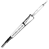
| + | Another driver takes care of running the X-Axis, which was implemented by a linear actuator that was kindly donated to the project by Szymon. It uses a somewhat old (and buggy!) serial-based controller unit (National Aperture MC-4B Series), for which I managed to dig up the manual from the Internet Archive, see here: {{ : | ||
| + | |||
| + | === Main Software and Algorithms === | ||
| + | |||
| + | The main laser microscope class provides a few methods for focus control and scanning a predefined area to an image file. The focusing is the most interesting aspect here. Generally, the focusing first performs a wide scan of the Z-height to find the linear region of the focus error detector. Following that, it implements a simple PI control scheme for successively minimizing the focusing error. | ||
| + | |||
| + | As relatively large scan areas should be possible, focus tracking during the scan is required. Initially, the software uses a relatively simple algorithm to achieve this: | ||
| + | | ||
| + | | ||
| + | * Least-Squares-Fit a 3D plane through all the points on the grid | ||
| + | * During the actual scan, calculate the optimal Z-height for a given position by evaluating the Z-Coordinate of this plane | ||
| + | |||
| + | Another noteworthy aspect is the Y-Axis (implemented using the DVD drive motor and mechanism). Given this whole mechanism is a made from a few cheap plastic pieces, | ||
| + | it has some backlash to it. This could be reliably solved by only approaching positions from one side. This yields surprisingly good repeatability (sub-µm-range), | ||
| + | |||
| + | The software is as open as everything else (though a little more hacky), and can be found in [[https:// | ||
| + | |||
| + | ===== Full System and Mechanical Assembly ===== | ||
| + | The following two pictures show the system fully assembled. Also below is a picture of the linear actuator used for the X-Axis. This is a wonderfully precise instrument (National Aperture linear stage with sub 100 nm positioning accuracy). Its only downfall is the controller (see my ramblings above in the Software | ||
| + | |||
| + | {{: | ||
| + | |||
| + | {{: | ||
| + | |||
| + | {{: | ||
| + | |||
| + | ===== Sample Preparation and Imaging ===== | ||
| + | With the full system in place, all that remains is to place a sample on the X-stage and start alignment and scanning. For sample preparation, | ||
| + | |||
| + | {{: | ||
| + | |||
| + | Alignment is a somewhat tricky process, but using the laser at low current (to produce a just-visible dot on the sample without causing any laser safety concerns) helps a great deal. | ||
| + | |||
| + | The scanning process can last from a few minutes to a few hours, depending on the required step size (quality) and area of the scan. Here's a few examples of resulting images: | ||
| + | |||
| + | |||
| + | |||
| + | Coarse imaging of some antique EPROM device, scan area 1x1mm. (Picture Below) | ||
| + | |||
| + | {{: | ||
| + | |||
| + | |||
| + | Higher resolution scan of the same device EPROM, scan area 500x500 um (top right of previous image). The two routing layers can be seen above one another. (Picture Below) | ||
| + | |||
| + | {{: | ||
| + | |||
| + | |||
| + | Scan of an I2C test chip from my colleague Szymon (fabricated in 65nm CMOS, picture below). Scan area 1x1mm. | ||
| + | |||
| + | {{: | ||
| + | |||
| + | This picture shows some of the aforementioned nonlinearity in one axis, which introduces periodical distortions in the image. These could be corrected in principle, but I didn't bother. The nice CERN logo was placed on the top metal layer, and some of the lower level metals are actually already visible from the top (the vertical and horizontal power distribution stripes are placed on the two metal layers below). | ||
| + | |||
| + | Also from this chip, here's a few very small scans performed at 200 nm step size. Small metal filling patterns on the top metal layer are imaged, each of which is only about a two micron wide square. Lithographic imperferfections can clearly resolved using this imaging technique. The horizontal (black) lines were caused by the erratic X-axis stage, sometimes going to places it was not told to go... | ||
| + | |||
| + | {{: | ||
| + | |||
| + | |||
| + | Finally, here are two videos of the device in Action: | ||
| + | * Focusing: https:// | ||
| + | * Scanning: https:// | ||
| + | |||
| + | ===== Summary ===== | ||
| + | For not a lot of money, a rather capable little laser microscope could be built. At some point, more scanned objects will be added to the collection above. If you are interested in replicating this project or a part of it, all developments are publicly available in the following repositories: | ||
| + | * Hardware: https:// | ||
| + | * FPGA Gateware: https:// | ||
| + | * PC software: https:// | ||
| + | |||
| + | ===== References ===== | ||
| + | I'm of course not the first one to build something like this. Here's some sources of my own inspiration: | ||
| + | * http:// | ||
| + | * https:// | ||
| + | | ||
| + | | ||
projekte/dvdlsm/start.1580075956.txt.gz · Zuletzt geändert: von thasti