projekte:dvdlsm:start
Unterschiede
Hier werden die Unterschiede zwischen zwei Versionen angezeigt.
| Beide Seiten der vorigen RevisionVorhergehende ÜberarbeitungNächste Überarbeitung | Vorhergehende Überarbeitung | ||
| projekte:dvdlsm:start [2021/02/07 00:28] – [OPU Modification] thasti | projekte:dvdlsm:start [2021/02/07 22:25] (aktuell) – [Laser Diodes, Lens and Actuators] thasti | ||
|---|---|---|---|
| Zeile 1: | Zeile 1: | ||
| ~~NOTOC~~ | ~~NOTOC~~ | ||
| - | ====== DVD-Drive-Based | + | ====== DVD-Drive |
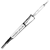
| - | {{ : | + | {{ : |
| Due to an abundance of one specific type of DVD drives, plans were made to give a useful afterlife to these devices. A laser scanning microscope seemed to be the most useful project. | Due to an abundance of one specific type of DVD drives, plans were made to give a useful afterlife to these devices. A laser scanning microscope seemed to be the most useful project. | ||
| Zeile 29: | Zeile 29: | ||
| ==== Laser Diodes, Lens and Actuators ==== | ==== Laser Diodes, Lens and Actuators ==== | ||
| - | The OPU houses two laser diodes. As this is just a DVD/CD reader, the lasers are not very powerful but provide sufficient power for microscopic | + | The OPU houses two laser diodes. As this is just a DVD/CD reader, the lasers are not very powerful but provide sufficient power for microscopy |
| The primary lens is positioned using electromagnetic actuators. These come in the form of three coils, which tilt or move the coil proportionally to the current flowing though them. Their polarity and required full-scale DC actuation current can be easily found by using a lab power supply. | The primary lens is positioned using electromagnetic actuators. These come in the form of three coils, which tilt or move the coil proportionally to the current flowing though them. Their polarity and required full-scale DC actuation current can be easily found by using a lab power supply. | ||
| Zeile 59: | Zeile 59: | ||
| It was conjectured that the smaller inner quadrants were responsible for the low-sensitivity outputs, while the outer segments would produce a large amplitude (due to their larger light collection area). | It was conjectured that the smaller inner quadrants were responsible for the low-sensitivity outputs, while the outer segments would produce a large amplitude (due to their larger light collection area). | ||
| - | In a second reverse engineering session, the exact pinout was determined by means of selective illumination: | + | In a second reverse engineering session, the exact pinout was determined by means of selective illumination: |
| {{: | {{: | ||
| Zeile 148: | Zeile 148: | ||
| - | Higher | + | Higher |
| {{: | {{: | ||
| - | Scan of an I2C test chip from my colleage | + | Scan of an I2C test chip from my colleague |
| {{: | {{: | ||
| - | This picture shows some of the aforementioned nonlinearity in one axis, which introduces periodical distortions in the image. These could be corrected in principle, but I didn't bother. The nice CERN logo was placed on the top metal layer, and is composed | + | This picture shows some of the aforementioned nonlinearity in one axis, which introduces periodical distortions in the image. These could be corrected in principle, but I didn't bother. The nice CERN logo was placed on the top metal layer, and some of the lower level metals |
| Also from this chip, here's a few very small scans performed at 200 nm step size. Small metal filling patterns on the top metal layer are imaged, each of which is only about a two micron wide square. Lithographic imperferfections can clearly resolved using this imaging technique. The horizontal (black) lines were caused by the erratic X-axis stage, sometimes going to places it was not told to go... | Also from this chip, here's a few very small scans performed at 200 nm step size. Small metal filling patterns on the top metal layer are imaged, each of which is only about a two micron wide square. Lithographic imperferfections can clearly resolved using this imaging technique. The horizontal (black) lines were caused by the erratic X-axis stage, sometimes going to places it was not told to go... | ||
| {{: | {{: | ||
| + | |||
| + | |||
| + | Finally, here are two videos of the device in Action: | ||
| + | * Focusing: https:// | ||
| + | * Scanning: https:// | ||
| ===== Summary ===== | ===== Summary ===== | ||
| Zeile 169: | Zeile 174: | ||
| * PC software: https:// | * PC software: https:// | ||
| - | + | ===== References ===== | |
| + | I'm of course not the first one to build something like this. Here's some sources of my own inspiration: | ||
| + | * http:// | ||
| + | * https:// | ||
| + | * https:// | ||
| + | * https:// | ||
projekte/dvdlsm/start.1612657689.txt.gz · Zuletzt geändert: 2021/02/07 00:28 von thasti